High-performance SiSiC plates for semiconductor machinery
With photolithography systems for semiconductor manufacturing becoming ever more sophisticated, component suppliers need to be able to provide products of the highest quality to meet the current and future demands in chip production. Based on ongoing in-house research and development, CeramTec’s “Rocar SiF” plates made of high-performance SiSiC as a lightweight silicon carbide ceramic achieve an optimal balance of material properties which contribute to higher chip quality.
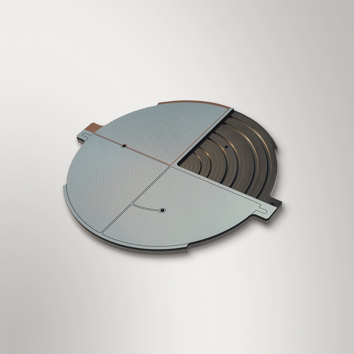
The company, a global leader in the production of advanced technical ceramics, provides SiSiC (silicon infiltrated silicon carbide) plates made of silicon carbide with a specific amount of metal silicon, which form the basis for electrostatic chucks. These wafer chucks are used in semiconductor machinery for the production of chips to accurately position the silicon wafer in the machine, employing an electrostatic field to clamp the wafer under vacuum conditions. Silicon carbide as the hardest ceramic material offers not only the stiffness and absolute flatness needed to enable this process but also excellent thermal conductivity as well as thermal shock, wear and corrosion resistance.
Material composition key for optimal use in semicon machinery
“Balancing the needs for a material that is highly homogeneous and refined while retaining the highest possible conductivity is a challenge when it comes to producing these plates,” explains Heiko Schulz, Sales Director Machinery at CeramTec. “Our Rocar SiF product is the result of years of research and ongoing development, providing our customers now with the ‘best of both worlds’: The material is as homogeneous as possible, meaning that the conductive free silicon portion is as evenly spread across the microstructure as possible and at the same time retains optimum conductivity. This enables high-precision microstructuring of the SiSiC surface and, ultimately, more accurate handling of the silicon wafer which has a direct impact on chip quality and obtainable chip structure.”
Component matching demands of latest manufacturing processes
Litography as the use of light to print tiny patterns on silicon is a fundamental step in mass-producing computer chips and a new generation of lithography machines now operates at the cutting-edge of what is physically possible. As a small but crucial component, CeramTec’s SiSiC plates undergo a finishing process before being incorporated in this highly advanced EUV (extreme ultraviolet) lithography systems used by computer chip makers, which make silicon features down to a few nanometers in size on the memory chips and processors of tomorrow to meet the growing demand driven by 5G, IoT or autonomous driving applications. “Our customers who perform this finishing process of adding customised patterns on the SiSiC plates benefit from the composition of our Rocar SiF material as it simplifies processability which ultimately shortens the very time-consuming refining procedure of the plates,” adds Heiko Schulz. Given the expected growth of worldwide semiconductor manufacturing equipment market which is already manifested in the increasing number of EUV lithography systems being installed, semiconductor industry suppliers can therefore benefit from working with a high-quality base material to increase efficiency and productivity.